The Semiconductor industry is evolving rapidly. Detecting defects in semiconductor wafers is crucial to ensure electronic components function correctly, and Semiconductor Wafer Defect Detection with AI boosts efficiency in achieving this goal.
Artificial intelligence (AI) is transforming this task. It is making defect detection faster. It is also making it more accurate than ever before.
Key takeways:
- Accurate defect detection: AI spots microscopic defects that humans often miss. This enhances product quality and cuts down on waste.
- Industry adoption proves results: Companies like TSMC benefit from faster inspections. AI enhances throughput and accuracy in real-world applications.
- Overcoming AI challenges: AI still faces integration and data issues. Ongoing improvements are making AI systems more efficient and adaptable in manufacturing.
- Common wafer defects: Defects such as clusters, surface imperfections, and scratches can harm wafer performance. They pose significant risks to manufacturing processes.
What is Semiconductor Wafer Defect Detection?
Semiconductor wafer defect detection with AI involves finding flaws in thin slices of semiconductor material. These slices serve as the foundation for electronic circuits. Early detection of these defects saves time and resources. It ensures high-quality production.
Types of Defects
Common types of defects include:
- Cluster: Groups of defects that appear together in localized areas of the wafer.
- Complex: Defects involving multiple layers or structures, affecting the wafer’s functionality.
- Edge: Flaws found along the wafer’s perimeter, often caused by handling or processing errors.
- Face: Surface-level imperfections that impact the wafer’s top layer, potentially disrupting the manufacturing process.
- Scratches: Physical marks that damage electrical pathways, leading to potential failures in the wafer’s performance.

Traditional Detection Methods
Before AI, wafer defects were detected through manual inspection. Inspectors used microscopes and optical tools. This method was slow. It was prone to human error. It lacked precision and varied between inspectors. These shortcomings highlighted the need for better solutions.
The Emergence of semiconductor wafer defect detection with AI
AI is changing wafer defect detection by offering speed, accuracy, and consistency. AI systems learn from thousands of defect images. They recognize patterns. They use computer vision to spot defects more efficiently than humans can.
Benefits of Using AI in Semiconductor Wafer Defect Detection
Increased Accuracy
Semiconductor wafer defect detection with AI detects minute defects that manual inspections often miss. This helps in improving overall product quality.
Faster Processing
AI analyzes images rapidly. This allows for real-time defect detection during manufacturing. It reduces downtime and prevents defective wafers from advancing.
Consistency and Reliability
AI provides consistent results, eliminating human variability. This reliability ensures thorough inspections and maintains high-quality standards.
Cost Savings
Early and accurate defect detection prevents unnecessary processing of defective wafers. This minimizes waste and optimizes resource utilization.
Industry Adoption Examples
Applied Materials
Applied Materials uses Cold Field Emission (CFE) technology combined with AI to enhance defect detection. This system provides sub-nanometer resolution. It detects the smallest defects, even those buried within advanced 3D structures.
AI helps extract and classify defects of interest (DOIs) from nuisance signals. This increases accuracy and reduces false alarms. The AI-enhanced system can handle up to 10,000 defect candidates in under an hour. This significantly boosts throughput and efficiency.

Taiwan Semiconductor Manufacturing Company (TSMC)
According to McKinsey’s report, TSMC uses semiconductor wafer defect detection with AI. It improves overall manufacturing efficiency. AI increases detection rates and significantly reduces inspection times. It helps TSMC enhance resilience in wafer manufacturing processes. This contributes to better production yields and reduced waste.
Challenges and Future Developments
AI in defect detection faces several challenges, including:
- High-Quality Data Requirements: AI needs large amounts of high-quality, labeled data. Collecting this data is costly and time-consuming, especially for advanced nodes. Without it, AI struggles to maintain accuracy and reliability.
- Integration Complexities: Integrating AI into existing workflows is challenging. Legacy systems often lack infrastructure for AI, requiring significant investments in hardware, software, and training.
- Interpretability Issues: AI’s “black box” nature makes its decisions hard to explain. This can slow adoption and create trust issues for engineers who don’t fully understand the defect flagging process.
- Scalability and Adaptability: As semiconductor tech evolves, semiconductor wafer defect detection with AI must adapt to new processes and materials. Frequent retraining is needed, making it resource-intensive to scale and keep up with industry demands.
Ongoing Solutions:
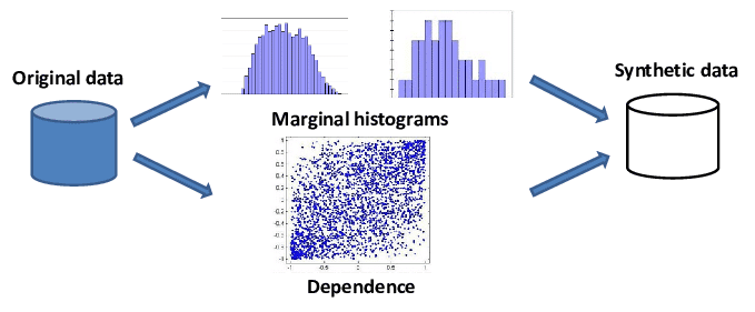
Researchers are utilizing synthetic data to supplement real-world datasets, helping AI models train with a wider range of scenarios and addressing the issue of data scarcity. In parallel, efforts to develop Explainable AI (XAI) are underway, which aim to make AI decision-making processes more transparent.
This fosters trust and makes it easier for engineers to adopt AI technologies. Additionally, industry groups are working to standardize AI integration methods, streamlining the process and allowing manufacturers to implement AI solutions without significant overhauls to their existing systems.


The Road Ahead
AI will continue to enhance wafer defect detection through several promising developments:
- Predictive Maintenance: AI can forecast defects by analyzing production data for patterns. This allows manufacturers to address issues before they occur, reducing downtime and improving overall production flow.
- Real-Time Process Optimization: AI continuously analyzes sensor data to spot bottlenecks and inefficiencies in manufacturing. It suggests parameter adjustments, such as temperature or alignment, to boost yields and enhance product quality.
- Human-AI Collaboration: While AI excels at speed and precision, human judgment remains vital for complex defects. Future systems will balance AI’s efficiency with human expertise in decision-making.
- Scalability for Next-Generation Architectures: AI must evolve to handle complex structures like GAA and 3D NAND. These require advanced defect detection, with future AI solutions likely incorporating quantum or high-performance computing to meet new demands.
Conclusion
Semiconductor wafer defect with AI is changing the industry forever. This transformation ensures higher product quality. It’s benefits include greater speed, accuracy, efficiency, and it also helps in reducing waste. It supports a more promising future for semiconductor manufacturing.

